1. Introduction: The Rise of Glass as a Packaging Substrate
For decades, silicon has been the dominant material for both active devices and, increasingly, for passive interposers in 2.5D and 3D advanced packaging. Silicon interposers – enabled by Through‑Silicon Via (TSV) technology – have successfully bridged the gap between logic chips and memory or I/O devices.
However, as packaging demands shift towards higher frequencies (millimeter‑wave 5G/6G), larger form factors (chiplets), and lower cost, a new contender has emerged: glass. Glass substrates offer a compelling combination of electrical, mechanical, and cost properties that make them an attractive alternative – or complement – to silicon interposers.
At the heart of glass interposer technology is the Through‑Glass Via (TGV) – a vertical electrical interconnection that passes through the glass substrate, connecting circuitry on the top and bottom surfaces. TGVs are the glass equivalent of TSVs, enabling high‑density, high‑aspect‑ratio vertical interconnects with superior high‑frequency performance.
This article provides a comprehensive guide to TGV technology: what it is, why glass substrates are advantageous, how TGV differs from TSV, and the critical role of laser drilling in creating these tiny, precise vias.
2. What Is Through‑Glass Via (TGV)?
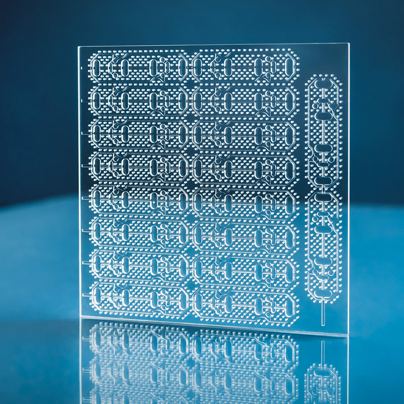
A Through‑Glass Via (TGV) is a fully metallised vertical hole that penetrates a glass substrate, providing an electrical path from one side of the glass interposer to the other. TGVs enable:
Vertical interconnection between stacked chips or between a chip and a package substrate.
Signal routing with ultra‑low insertion loss and negligible cross‑talk.
Power delivery with reduced parasitic capacitance.
Thermal dissipation (glass is a moderate thermal conductor, and vias can be filled with copper to aid heat spreading).
2.1. TGV Structure
A typical TGV consists of the following key structural elements:
| Component | Description |
|---|---|
| Glass substrate | Alkaline‑free or borosilicate glass, typically 100–500 µm thick, with CTE matched to silicon (for chip stacking) or to organic substrates (for fan‑out). |
| Via hole | A cylindrical or tapered hole through the glass – typically 30–100 µm in diameter, with aspect ratios (depth:diameter) of 5:1 to 20:1. |
| Barrier / adhesion layer | Thin films (e.g., Ti, TiW, or Cr) deposited on the via sidewall to promote adhesion of the subsequent conductive layer. |
| Seed layer | Copper or other metal deposited by sputtering or electroless plating to enable electrolytic copper fill. |
| Copper fill | Fully plated copper filling the via, providing the electrical connection. |
The quality of the via hole – smooth sidewalls, vertical profile, no micro‑cracks, and no debris – is paramount. This is where the drilling method determines the ultimate reliability and electrical performance of the TGV.
3. Glass Substrate Advantages: Why Glass Over Silicon?
Glass interposers are not simply a drop‑in replacement for silicon – they offer distinct advantages in several key areas:
| Property | Glass Substrate | Silicon Substrate |
|---|---|---|
| Dielectric constant (Dk) | ~4.8 (low, stable over frequency) | ~11.9 (much higher) |
| Loss tangent (Df) | 0.002–0.005 (very low) | 0.01–0.02 (higher loss) |
| Electrical resistivity | >10¹⁴ Ω·cm (excellent insulator) | ~10³ Ω·cm (semiconductor – requires insulation layer) |
| Thermal expansion (CTE) | 3–8 ppm/°C (tuneable to match Si or organics) | 2.6 ppm/°C (fixed) |
| Mechanical stiffness | Lower than silicon – can be beneficial for warpage control | Stiffer – more prone to warpage |
| Cost | Low (large‑area panels up to 500×500 mm) | High (300 mm wafer, limited panel size) |
| Surface roughness | Extremely smooth (sub‑nm) – ideal for fine‑line RDL | Moderate – requires CMP |
| High‑frequency performance | Excellent – minimal dielectric loss, low cross‑talk | Inferior – high loss, parasitic capacitance |
| Transparency | Transparent – useful for optical alignment | Opaque |
3.1. Key Differentiators
High‑frequency / RF performance: For 5G, radar, and high‑speed digital applications (≥30 GHz), glass's low Dk and Df translate to significantly lower insertion loss and better signal integrity than silicon.
Large‑area panel processing: Glass can be processed on large panels (Gen 2, Gen 3) rather than 300 mm wafers, dramatically reducing cost per interposer.
CTE tuneability: Glass manufacturers can adjust the coefficient of thermal expansion to closely match silicon chips (to minimise thermo‑mechanical stress) or organic substrates (to reduce warpage in fan‑out packages).
No insulation layer required: Unlike silicon, which requires a thick oxide insulation layer to isolate vias from the substrate, glass is inherently insulating – simplifying the fabrication process.
4. TGV vs. TSV – A Side‑by‑Side Comparison
While TGVs and TSVs serve the same fundamental purpose – vertical interconnection – they differ significantly in materials, fabrication processes, and performance.
| Parameter | Through-Glass Via (TGV) | Through-Silicon Via (TSV) |
|---|---|---|
| Substrate Material | Borosilicate / Quartz / Alkaline-Free Glass | Single-Crystal Silicon |
| Substrate Isolation | Not required (native electrical insulator) | Required (SiO₂/SiN dielectric liner required) |
| Via Formation Method | Ultrafast Laser Drilling / Laser-Induced Etching | Bosch Deep Reactive Ion Etching (DRIE) |
| High-Frequency Parasitomics | Ultra-low insertion loss & parasitic capacitance | Higher parasitic capacitance & high-frequency attenuation |
| Form Factor Scalability | Panel-level manufacturing (500×500mm+) | Wafer-level manufacturing (Max 300mm round) |
5. Laser Drilling for TGV – The Critical Enabling Technology
The creation of the via hole is the most demanding step in TGV fabrication. Unlike silicon, which can be etched by DRIE, glass is chemically inert to most standard etchants (except HF, which is hazardous and isotropic). Therefore, laser drilling has become the primary method for creating TGVs.
5.1. Why Laser Drilling?
| Advantage | Explanation |
|---|---|
| Mask‑less | Direct digital patterning – no photomasks or lithography required. |
| Substrate‑independent | Works on any glass type, thickness, or surface finish. |
| High‑aspect‑ratio capability | Can produce deep, narrow vias with controlled taper. |
| Low thermal damage | Ultrafast lasers (ps/fs) achieve cold ablation – no micro‑cracks or melting. |
| High throughput | Galvo scanners and multiple beams enable fast processing. |
| Integration | Can be combined with subsequent cleaning, metallisation, and RDL steps in a single production line. |
5.2. Laser Source Selection for TGV Drilling
The choice of laser wavelength and pulse duration is critical for TGV quality. The vast majority of industrial TGV drilling is performed with ultrafast lasers – specifically picosecond or femtosecond UV or near‑IR lasers.
| Laser Type | Wavelength | Pulse Width | Suitability for TGV | Remarks |
|---|---|---|---|---|
| CO₂ | 10.6 µm | µs | Not suitable | Thermal melting, creates micro‑cracks, HAZ >100 µm, poor sidewall quality. |
| IR nanosecond | 1064 nm | ns | Not recommended | Glass absorbs poorly; energy couples via nonlinear effects but causes chipping. |
| UV nanosecond | 355 nm | ns | Moderate | Better absorption but still thermal; may cause micro‑cracking in high‑aspect‑ratio vias. |
| UV picosecond | 355 nm | <10 ps | Excellent | Cold ablation, minimal HAZ, smooth sidewalls, high aspect ratio capability. |
| IR picosecond | 1064 nm | <10 ps | Very good | Nonlinear absorption in glass, deeper penetration, but beam quality may be lower than UV. |
| Femtosecond | 343–1064 nm | <500 fs | Outstanding | Ultimate quality, but slower and higher cost; used for R&D and ultra‑high‑reliability. |
Practical recommendation: For high‑volume, cost‑effective TGV manufacturing, UV picosecond (355 nm) lasers offer the best balance of via quality, throughput, and equipment cost. They produce vias with taper angles <2°, sidewall roughness <0.5 µm, and no micro‑cracks – meeting the stringent requirements of advanced packaging.
Chanxan Solution Spotlight
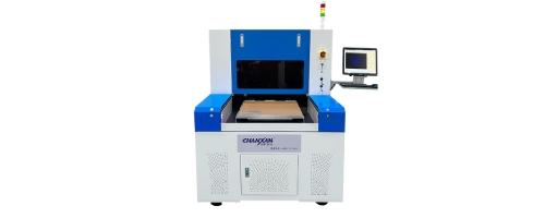
The Chanxan CW‑6050PZ Picosecond Laser System (355/1064 nm) is specifically engineered for glass TGV drilling, delivering exceptional via quality at mass-production speeds. Its ultra‑short pulse duration (<10 ps) guarantees precise cold ablation without micro-cracks or heat damage.
6. Process Parameters for High‑Quality TGV Drilling
Achieving consistent, high‑quality TGVs requires careful optimisation of key optical and motion parameters:
| Parameter | Recommendation for TGV Drilling |
|---|---|
| Pulse energy | Typically 10–50 µJ per pulse – adjusted for glass thickness and target via diameter. |
| Spot size | 10–30 µm – smaller spots produce finer vias but require more passes. |
| Scanning strategy | Trepanning (spiral) is preferred – it gradually removes material from the centre outward, producing vertical sidewalls with minimal taper. |
| Number of passes | 10–50 passes, depending on glass thickness and pulse energy. Each pass removes 2–5 µm of material. |
| Repetition rate | 200–800 kHz – high rep‑rate increases throughput but may cause heat accumulation; balance with scan speed. |
| Scan speed | 100–500 mm/s – slower speeds improve material removal per pass but reduce throughput. |
| Focus position | Dynamic Z‑tracking is essential – the focus must move down as the via deepens to maintain constant fluence. |
| Assist gas | Dry air or nitrogen at 1–2 bar to remove debris; helium is sometimes used for better debris evacuation. |
| Cleaning | Post‑drill cleaning (ultrasonic or wet chemical) removes residual glass particles and prepares sidewalls for metallisation. |
Key Quality Indicators:
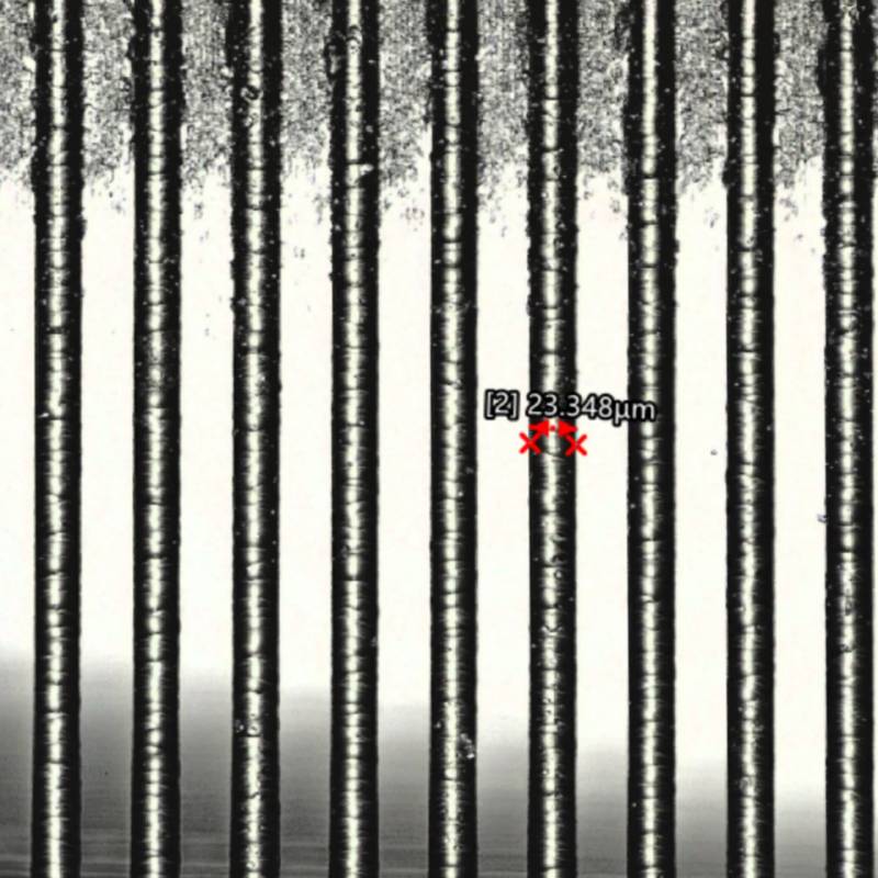
Sidewall roughness (Ra): ≤0.5 µm (smooth enough for barrier layer deposition).
Taper angle: ≤2° (near‑vertical).
Micro-cracks: Zero micro‑cracks (verified by cross‑section SEM).
Debris: Zero debris or redeposition (inspected by optical microscopy).
7. The Complete TGV Fabrication Flow
A typical TGV glass interposer process sequence involves nine primary stages:
Glass substrate preparation: Cleaning, optionally thinning or polishing.
Laser drilling: Create via holes using UV picosecond laser trepanning.
Cleaning / etching: Remove laser‑induced debris and micro‑roughness (dilute HF or plasma cleaning).
Barrier / adhesion layer deposition: Sputtering of Ti, TiW, or Cr (50–200 nm).
Seed layer deposition: Sputtered copper (200–500 nm).
Electrolytic copper filling: Bottom‑up plating to fully fill the vias.
Planarisation: Chemical‑mechanical polishing (CMP) or grinding to remove overburden copper.
Redistribution layer (RDL) formation: Lithography and plating for fan‑out routing.
Thinning (optional): Backside grinding to expose TGVs if needed.
Laser drilling is the first and most critical step – the quality of the via determines the yield of all subsequent steps.
8. Quality Assurance and Defect Mitigation for TGV
| Defect | Cause | Solution |
|---|---|---|
| Micro‑cracks around via entrance | Excessive pulse energy or thermal accumulation | Reduce pulse energy; increase scan speed; use picosecond (cold ablation). |
| Tapered / conical sidewalls | Insufficient dynamic focus adjustment | Implement real‑time Z‑tracking to maintain focus depth. |
| Debris / redeposition inside via | Incomplete debris evacuation | Increase assist gas pressure; add post‑drill cleaning step. |
| Hole not through (incomplete) | Insufficient number of passes or low energy | Increase passes or pulse energy; verify glass thickness. |
| Sidewall roughness >1 µm | Too high pulse overlap or incorrect focal position | Adjust hatch overlap; re‑optimise focus; use smaller spot size. |
| Glass chipping at via exit | High energy breakout pulse | Reduce energy for final passes; use a tapered exit strategy. |
Inspection Methods: Cross‑sectioning + SEM, optical microscopy, and infrared transmission inspection (glass is transparent) are used to verify via quality before metallisation.
9. Conclusion: TGV – The Future of High‑Performance Interposers
Through‑Glass Via technology represents a paradigm shift in advanced packaging. By replacing silicon with glass as the interposer substrate, manufacturers can achieve:
Superior high‑frequency performance: Critical for 5G, automotive radar, and optical transceivers.
Larger form factors: Enabling chiplet integration and system‑in‑package designs.
Lower cost: Through panel‑scale processing and fewer processing steps.
Better electrical isolation: No parasitic capacitance to the substrate.
The success of TGV hinges on the quality of the via drilling process. Here, ultrafast laser technology – particularly UV picosecond lasers – provides the precision, speed, and substrate integrity that traditional thermal or mechanical methods cannot match.
Chanxan Dedicated TGV Solution
The Chanxan CW‑6050PZ Picosecond Laser System(UV/IR) is purpose‑built for high‑aspect‑ratio TGV drilling in glass substrates. Its ultra‑short pulse duration (<10 ps) delivers cold ablation with no micro‑cracks, no melting, and no carbonisation – producing vias with smooth, vertical sidewalls and excellent repeatability.
With Chanxan's CW‑6050PZ, manufacturers can transition from R&D prototyping to high‑volume production of glass interposers with confidence – achieving the via quality, throughput, and yield demanded by next‑generation advanced packaging applications.